Foundry Services
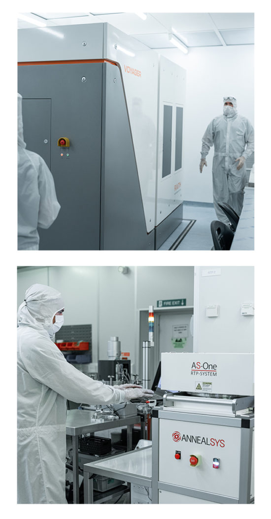
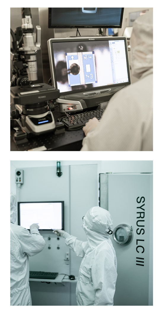
Our foundry provides end-to-end design, manufacture and qualification for early phase prototypes and high-volume production, supporting up to 100mm wafer sizes on InP, GaAs, GaSb and GaN substrates. We have an extensive portfolio of unique production process IP, essential to high-quality, reliable, volume manufacturing.

Front-End Foundry Capability
Epitaxial Growth
MOCVD |Regrowth and overgrowth qualified processes
Lithography
Stepper | Contact Aligner | E-beam
Etching
ICP | RIE | Wet
Metallisation
Sputtering | Evaporation | Electroplating
Dielectric Deposition
PECVD | Sputtering
|
|
|
|
|
|
|

Back-End Foundry Capability
Optical Facet Coating
AR | HR | ULAR | On wafer & laser bar
Testing
High volume electro/optic test capacity | 2M lasers per month
Singulation & Visual Inspection
High volume automated manufacturing
Device Qualification
HTOL | ALT | Damp-Heat | Supporting Telcordia GR-468 and beyond
Read about the latest investment into our fab:
|
|
|
|
|
Contact Sivers Photonics
For more information about Sivers Photonics, or to discuss your Photonics project requirements.